
Master Course for Fluid Simulation Analysis of Multi-phase Flows by Oka-san: 6. Free surface flow analysis V
Free surface flow analysis V
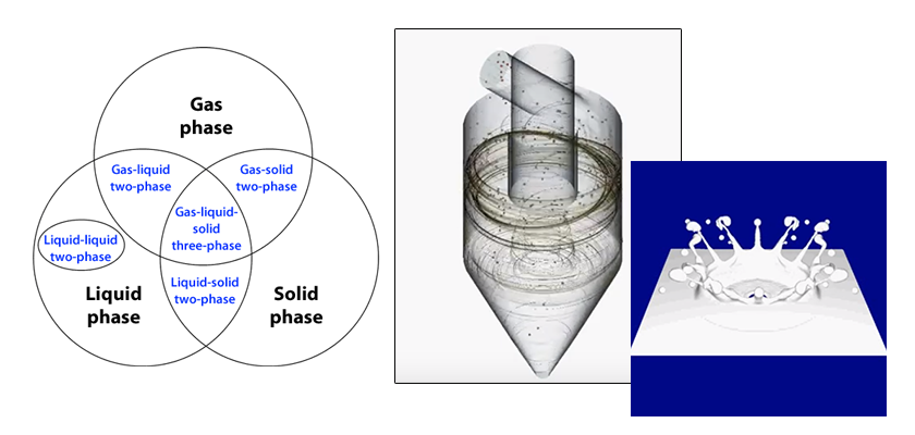
This section looks at an example of a micro scale free surface flow.
Modern electronic devices such as smartphones. Electronic components smaller than 1 mm in size are densely mounted on a circuit board. Mass production of these densely-mounted electronic components cannot be achieved by soldering the components to the board by hand. Instead, solder paste (solder cream) is applied to the board with a printing machine and electrical components are attached to it. Then, the entire assembly is heated and cooled, and the solder paste melts and solidifies. This mounting process is called reflow soldering.
In this section, the behavior of molten solder used for reflow soldering is analyzed using the VOF method. As shown in Figure 1, solder cream is applied to the two lands on the board, and a square-shaped chip resistor is attached. The size of the resistor is 0402 (0.4 mm long, 0.2 mm wide). In this analysis, the viscosity of the molten solder is changed from 100 to 0.020 and from 0.020 to 100 (Pa・s) as it heated and cooled. The density of the solder is 8,000 kg/m3. Its surface tension is 0.40 N/m. The contact angle between the lands and the chip resistor is 30 degrees.
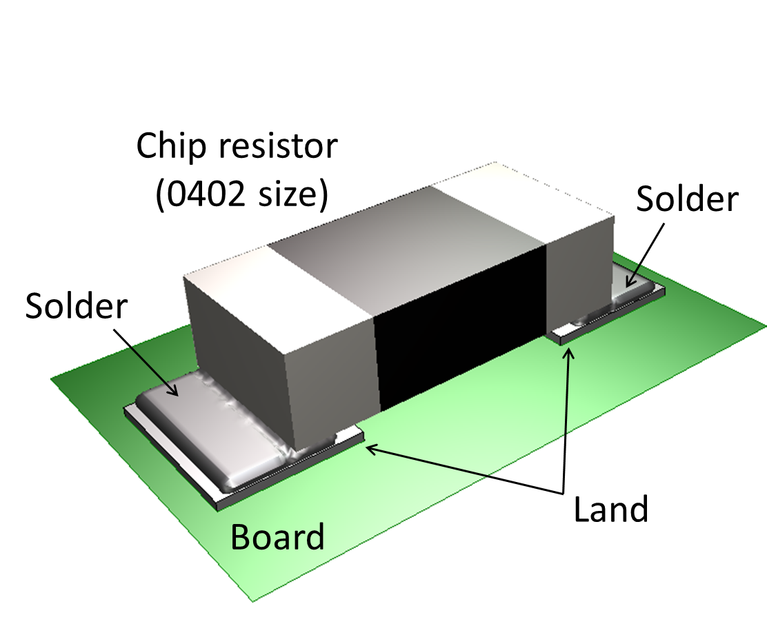
Figure 1: Chip resistor
The overset mesh is used in the moving overlap region that surrounds the chip resistor and each element in the static region as shown in Figure 2. The translation and rotation of the chip resistor as the solder melts and solidifies is solved by using the six-degrees-of-freedom equations of motion and the force applied by the solder.
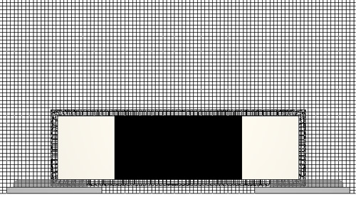
Figure 2: Overset mesh
Figure 3 shows the analysis result for the solder surface. As shown in Figure 3, the formation of solder fillets at both ends of the chip resistor is properly captured by the simulation. Figure 4 shows the front view of the fillets.
Figure 3: Surface of molten solder (without misalignment)
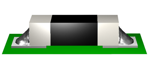
Figure 4: Solder fillet (without misalignment)
Figure 5 shows the top of the chip resistor. The resistor is misaligned. Figure 6 shows the surface of molten solder with misalignment and Figure 7 shows the solder fillet with misalignment. These figures show that slight misalignment of the chip resistor does not cause any problem with fillet formation.
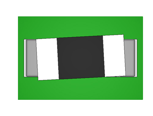
Figure 5: Top of chip resistor (with misalignment)
Figure 6: Surface of molten solder (with misalignment)
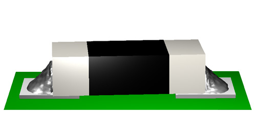
Figure 7 Solder fillet (with misalignment)
The next analysis looks at two types of horizontal misalignment of the chip resistor (Condition 1 and 2). These are analyzed as shown in Figure 8. There is no misalignment in the slanted direction. Figure 9 shows the surface of the molten solder for Condition 1, and Figure 10 shows solder fillets for Condition 1. As shown in Figure 9, the chip resistor shakes from side to side as the solder melts and solidifies, however; slight horizontal misalignment does not affect the formation of the solder fillets.
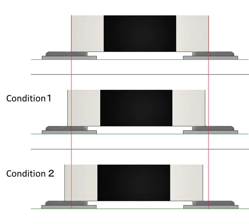
Figure 8: Horizontal misalignment (Condition 1, Condition2)
Figure 9: Surface of molten solder (Condition 1)
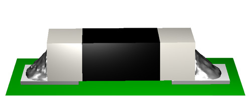
Figure 10: Solder fillet (Condition 1)
Figure 11 shows the surface of the molten solder for Condition 2. As shown in Figure 11, the phenomenon that causes electronic parts to stand is called the Manhattan phenomenon (also called chip-standing phenomenon). This name is used because the standing chips look like high-rise buildings in Manhattan section of New York. The fluid simulation properly reproduces the Manhattan phenomenon.
Figure 11: Surface of molten solder (Condition 2)
A couple of different examples have been used to illustrate free surface flow analyses. An almost infinite number of different analysis possibilities exist, but the two examples used here show how the latest fluid simulation analyses capabilities can be applied to different free surface applications ranging from micro scale to macro scale objects.
The next section will discuss particle tracking.

About the Author
Katsutaka Okamori | Born in October 1966, Tokyo, Japan
He attained a master’s degree in Applied Chemistry from Keio University. As a certified Grade 1 engineer (JSME certification) specializing in multi-phase flow evaluation, Okamori contributed to CFD program development while at Nippon Sanso (currently TAIYO NIPPON SANSO CORPORATION). He also has experience providing technical sales support for commercial software, and technical CFD support for product design and development groups at major manufacturing firms. Okamori now works as a sales engineer at Software Cradle.